United States Patent 6,920,540
Hampel, et al. July 19, 2005
Timing calibration apparatus and method for a memory device signaling system.
Abstract
A memory system includes a memory controller and a memory component coupled to each other. An interface of the memory component is configured to receive a first signal from the memory controller with read request information, retrieve the read data information from the memory core in response to the request information, and transmit to the memory controller a second signal containing the read data information. The read data information includes read data symbols, where the average duration of the read data symbols, measured at the interface, defines a symbol time interval. A first external access time is measured at the interface between a first read request and read data transmitted by the interface in response to the first read request. A second external access time interval is measured at the interface between a second read request and read data transmitted by the interface in response to the second read request. The difference between the first external access time and the second external access time is greater than one-half of the symbol time interval.
Inventors: Hampel; Craig E. (San Jose, CA); Perego; Richard E. (San Jose, CA); Sidiropoulos; Stefanos S. (Palo Alto, CA); Tsern; Ely K. (Los Altos, CA); Ware; Fredrick A. (Los Altos Hills, CA)
Assignee: Rambus Inc. (Los Altos, CA)
Appl. No.: 278478
Filed: October 22, 2002
United States Patent 6,920,402

Liaw, et al. July 19, 2005
Technique for determining performance characteristics of electronic devices and systems.
Abstract
A technique for determining performance characteristics of electronic devices and systems is disclosed. In one embodiment, the technique is realized by measuring a first response on a first transmission line from a single pulse transmitted on the first transmission line, and then measuring a second response on the first transmission line from a single pulse transmitted on at least one second transmission line, wherein the at least one second transmission line is substantially adjacent to the first transmission line. The worst case bit sequences for transmission on the first transmission line and the at least one second transmission line are then determined based upon the first response, and the second response for determining performance characteristics associated with the first transmission line.
Inventors: Liaw; Haw-Jyh (Fremont, CA); Yuan; Xingchao (Palo Alto, CA); Horowitz; Mark A.
(Menlo Park, CA)
Assignee: Rambus Inc. (Los Altos, CA)
Appl. No.: 799516
Filed: March 7, 2001
 United States Patent 6,919,749
Alon, et al. July 19, 2005
Apparatus and method for a digital delay locked loop.
Abstract
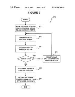
A circuit and method is shown for digital control of delay lines in a delay locked loop (DLL) system. A pair of multiplexors (MUXes) is used to select output taps from a pair of complementary delay lines that delay a reference clock signal in order to lock onto a received clock signal. An output tap from one delay line is used to produce a rising edge in an output clock signal while a corresponding tap in the complementary delay line is used to produce a falling edge in the output signal in order to correct for distortion. The MUXes are controlled based on a phase difference detected between the received clock signal and a feedback clock corresponding to the output clock signal. Another aspect of the present invention provides for generation of a quadrature clock by interpolating between the rising and falling edges selected for the output clock signal. Still another aspect of the present invention provides for selectively disabling unused elements of the delay lines to reduce power consumption.
Inventors: Alon; Elad (Saratoga, CA); Best; Scott (Palo Alto, CA)
Assignee: Rambus, Inc. (Los Altos, CA)
Appl. No.: 658710
Filed: September 8, 2003


No comments:
Post a Comment